Creating PCBs with the toner transfer method
There are many webpages explaining how to create printed circuit boards (PCBs) without having to use UV light and photoresist. However, most of them are bloated, unsurveyable or incomplete. This page is an attempt to document the process in a concise way.
Requirements
- A blank PCB, without a photoresist layer. If you only have boards with such a layer, you need to remove it first with a solvent like acetone.
- A type of paper, coated with a thin wax-like layer on one side, and easily dissolvable in water. Most inkjet ‘photo-paper’ is good. Some are better than others. Some companies like PulsarProFX produce special toner-transfer paper which has a kind of sugar-based coating. The toner sticks to this coating, which dissolves completely when soaked in water. The result is a very clean transfer that can also be used to transfer colour laser prints onto various surfaces. The method can also be extended to produce decals that will stick to about any surface, even curved. However, this paper is pretty expensive and hard to get outside the US.
- A laser printer with ordinary toner, 600dpi is recommended.
- A clothes iron.
- Acetone.
- A kind of abrasive sponge, like a scotchbrite pad, or steel wool. Some people say that steel wool may contaminate the copper, but others have used it without problems.
- Paper towel
- A toothbrush or similar semi-soft brush
- An etchant. The traditional etchant for copper is Ferric Chloride, but a cheap and very good alternative is a mixture of Hydrogen Chloride (HCl) and Hydrogen Peroxide (H2O2). Contrary to FeCl3, it's completely transparent, and very cheap (depending on where you get the chemicals).
- Safety goggles and gloves.
Method
Creating the design
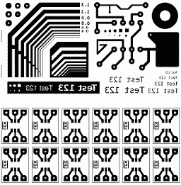
Your final PCB design should consist of a mirrored black-and-white bitmap of the copper pattern of the bottom of the PCB. This can be made in any way, ranging from the output from an expensive professional program to something you draw in the GIMP. A 300dpi image will do fine, anything above 600dpi is overkill.
Strictly spoken, holes are not necessary because you'll drill them anyway, but small holes in your design will make drilling a lot easier, first because you can see where to drill and second because the small hole in the copper will ‘guide’ the drill when biting into in the PCB. For this last effect to work, you should keep holes small, I use a diameter of 1/60" (0.42mm or 5 pixels in a 300dpi image).
Speaking about holes, if you're going to drill them manually, try to align as many holes on the same lines parallel with the edges of the PCB as possible. This will make it a lot easier and faster to drill them with a drill press, if it has a guide system (improvised or built-in).
Theoretically, everything you can print in a 300dpi image can end up as a copper trace, pad or letter on your print. In practice, anything thinner than 2/300 inch (2 pixels in a 300dpi image, or 0.17 mm) can be problematic. Avoid using 1/300 inch lines or spacings for structures that are supposed to conduct electricity.
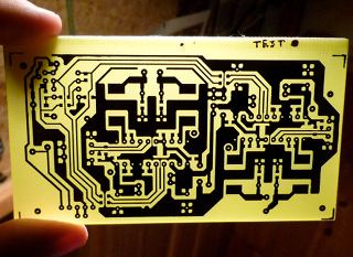
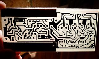
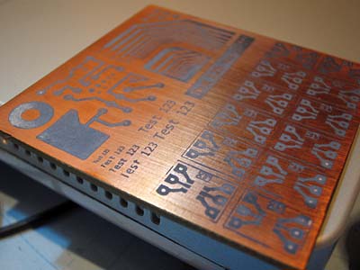
1/300 inch lines may actually work if you keep them away from the edges of the PCB. It is harder to properly transfer the toner near the edges. Therefore as a general rule, either avoid putting any fine structures near the edges, or cut the PCB to a size slightly larger than required for the design, and saw off the redundant parts after the transfer. Fine edges may smear, and/or not stick. You can see this below in the photos of the test PCB I made, of which the design is shown above.
If you're going to create a double-sided PCB, you will need to include some reference points that match on both sides. It is a good idea to include the edges of the PCB, but you may also put some extra marks outside the PCB area. This will make it easier to verify that the patterns are still aligned once you have sandwiched the PCB between them. You can slightly reduce the need for perfect alignment by making the ‘via’ solder pads of one of the sides slightly larger and not drawing holes in them.
Printing the design
It is kind of pointless to give you a list of good types of paper because manufacturers tend to change them at random moments. Nevertheless, some types that have been reported to work well are the “Picture Paper” from Staples in the USA, and the HEMA 170g “Photo paper” for people living in Belgium or the Netherlands. Brian reported me that he tried the Staples “Photo Supreme Gloss Paper - Inkjet compatible” instead of the basic paper and it was terrible, so there is certainly a lot of variation between different papers. I personally tried photo paper from a brand called ‘Ednet,’ and it worked reasonably well. However, I also tried the HEMA paper and it is indeed much better. Strictly spoken you don't need to use this photo-type paper, if you can find some plain office paper that dissolves very well in water, it should work too. Generally however, office paper dissolves poorly (nobody wants paper that dissolves the instant someone spills coffee on it).
Brian also reported great success with using the ‘waxed’ backing paper used for stickers and labels, like Avery labels. Remove all labels and print on the greasy side of the backing paper. Surprisingly, the toner sticks to this surface, even though I suspect that not all types of backing paper will work. I believe there is a risk that the toner will detach inside the printer and pollute the drum, so try this at your own risk.
You must print the design on the glossy side of the photo paper. Do not touch this side before or after printing. Remember, the design must be mirrored compared to what will be visible on the copper side of the PCB. Most laser printers allow to adjust the ‘density’ of the toner. If the printer has an LCD display, this setting can probably be found in its menu, or it can be adjusted with a software tool. By setting the density to maximum, more toner is deposited on the paper, which is what we want. (Don't forget to reset this setting to normal before printing a 100 page book :))
To avoid that the printer gets jammed by the rather thick paper, you must use the manual feed. It may be a good idea to print at least 2 copies of your design on the same page, so if you screw up the first one, you have a back-up handy. You may also want to print several designs on the same page to use the rather expensive photo paper more efficiently. But normally, the manual feed will allow to use smaller sizes of the paper than A4 or Legal, so you can re-use leftovers.
Some people say that sending the paper through the printer a second time (without actually printing anything, except a tiny dot or line to force the printer to warm up the drum) improves the quality of the transfer, but if you use good paper this should be unnecessary.
If you don't have access to a laser printer, you can also go to a copy center and make a copy of your print. Again, try to set the toner density to maximum and try not to anger the owner of the shop by jamming his machines with the thick paper :)
As I said in the intro, a specialized toner transfer paper is available that uses a sugar-based coating. In theory it should be possible to make similar paper yourself by brushing a water-sugar mix onto regular paper. I have tried to make such paper myself, but it proves to be hard to get the sugar solution right and apply a uniform thin coating. My first attempts produced paper that remained sticky even after days of drying. Feeding sticky paper to a laser printer would be a huge no-no. I then tried adding salt to the solution, which did eliminate the stickiness, but the toner didn't stick properly anymore. There is probably an optimal mix of sugar and salt, and perhaps adding starch to the mix could help as well, but it would take more experiments to find it.
Someone actually figured out a method to make good home-made transfer paper, but the method is pretty convoluted and time-consuming. If you're interested and have enough spare time, search for the text “How to Make Laser Toner Transfer Paper” by Triston J. Taylor.
Preparing the PCB
If the copper of the PCB appears to have oxidized a bit, first wash it with a bit of vinegar (or a stronger acid like HCl), which will return the metal to an un-oxidized state.
Scrub the copper side with the abrasive pad until the copper is shiny and clean.
Next, scrub the copper side with a paper towel soaked in acetone. This step is essential! The acetone will remove any remaining dirt and grease. If there's anything left on the copper, the toner won't stick well at those places. You should rub very hard on every square millimeter of the copper, switching to clean parts of the towel regularly. Repeat until no more dirt shows up on the towel. Needless to say, you must avoid touching the copper after this step.
Performing the actual toner transfer
Cut out the design, leaving only minimal margins except on one side. To make things easier, you can cut at least two sides of the paper so they match up with the sides of the PCB. This makes alignment trivial.
Double-layered boards are tricky and I have not yet tried to make any, but here are some possible strategies. The safest method would be to first transfer one side, and etch it with the other side protected by tape or foil. Also drill at least a few via holes to make alignment easier. Then transfer and etch the other side (again, covering the already etched side). Quicker but more difficult is to do both transfers at once, by sandwiching the pcb between the two sheets. Alignment could be problematic in this case. What could work, is to align the two sheets in advance. Hold them against a bright light and once aligned, stick or staple one or two edges together. Then you can insert the board in between and iron both sides.
Set the iron to its highest setting. Place the PCB, copper side up, on a heat-resistant surface. Wood will do, if you don't mind it getting a bit darker at one spot. Place the design on the copper (obviously with the toner facing down), aligning it properly. Then, while ensuring that the paper doesn't shift, place the hot iron on top of it. Press hard and move the iron around every 5 seconds, to ensure that the entire board is heated evenly. Next, rub the entire board with the sides and tip of the iron. Hold the iron slightly tilted so most of the pressure is concentrated on the tip. The paper should start to look shiny at those places you've already rubbed, so you can see which areas you still need to cover.
It's OK if the paper gets a little brownish during this whole process, this just means you're really heating it, which is good. It requires some experience to find the right amount of pressure required: too little pressure will cause a bad transfer, too much will cause the toner to smear out. Don't expect your first PCB to be perfect!
A better way to perform the toner transfer would be to use a laminator like the one used in laser printers: a roller which is heated and presses down on the paper with a large force. This would be quick, easy and produce a consistent quality. Unfortunately you'll have a hard time finding a laminator which allows a hard and thick PCB between its rollers. If you're handy, you might be able to make your own. Theoretically it could even be possible to modify a laser printer to accept the thick unbendable blank PCBs and print directly on them, but that would require overcoming a huge amount of obstacles and probably also pre-heating the PCB. Some people have successfully run a piece of aluminium foil through a laser, so printing on a metal surface should be possible despite the reliance on electrostatic charges to make toner stick to the drum.
Paul, a reader of this article, reported a large improvement in making the toner adhere to the blank PCB, by spraying the copper with a fine coat of a product called “Clean Screen”, right before placing the design on top and performing the transfer. The reason why this works might be that the product slightly dissolves the toner, making it more sticky. I tried a generic window cleaning product myself, and although I'm not sure whether it had any positive effect, the transfers were perfect, so it certainly doesn't hurt.
Removing the paper
Drop the board in a tub or sink with hot water (just not too hot to put your hands in). Let it soak for at least 10 minutes. Then you should be able to peel off the first layers of the paper. If you have trouble getting through the first layer, rubbing it with the toothbrush can help. As soon as you reach a dry layer, let it soak again. Eventually you will reach the last layer, which will be the ‘glossy’ one. This is often a bit nastier to get off. The toothbrush is the best tool for this job. Just rub until the layer breaks, and then continue rubbing until it comes off. If you did the ironing step well, you can rub pretty hard without damaging the toner. For really stubborn parts like the space between parallel traces, you can break the glossy layer with a needle.
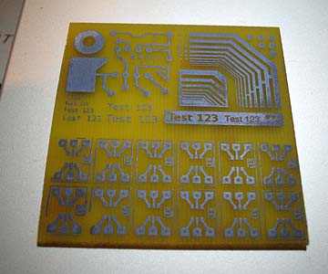
If you think all the paper has been removed, you can let the board dry. If any of the glossy layer still remains inside small holes or between nearby traces, it will show up as white (see bottom right of the image at the right). You can either soak the board again and rub those areas with the brush, or use a needle to remove the white areas, even when they're dry. It's no problem if there's some of the layer left on top of the toner areas, so don't bother rubbing it off.
In case a part of the toner doesn't stick to the copper, don't panic. If it's not a too large or delicate part, you can repair it with a good permanent marker. If you apply a sufficiently thick layer of ink, it should survive the etching process.
If on the other hand the toner is smeared out, you may have exerted too much pressure during the ironing step, the paper may be bad, and/or you may need to try using a lower toner density setting on your printer.
If at some point things go wrong (e.g. too much toner comes off or there is too much smearing), you can remove the toner with acetone, and start over (no need to scrub again, but you may need to remove oxidisation with some acid). Toner coming off can be due to bad paper, insufficient cleaning with acetone, or insufficient heat/pressure from the iron. If after repeated attempts it still won't work, try a different type of paper.
Etching
Whatever etchant you use, you should wear safety gloves, because you don't want to get any substance that dissolves metal on your skin. Safety goggles are also a good idea to prevent accidental splashes from getting in your eyes. It's obvious that you can't use a metal container to perform the etching. Especially aluminium with a HCl-based etchant is a very, very bad idea unless you're aching to get into massive trouble. If you want to know why, pour a little HCl in a glass jar in a well-ventilated area and drop a tiny ball of aluminium foil in it. Enjoy!
I can recommend the HCl+H2O2 mixture which works incredibly well, is transparent, and is also very cheap. On forums I found that the ideal proportions of (pure) H2O2, HCl and water are respectively 2/8/90. You'll need to divide the first two numbers by the concentration of the chemicals you can buy, and adjust the third one so they add up to 100. For instance, I could buy 27.5% H2O2 and 30% HCl at a general store, so I had to mix 7.3/26.7/66.
To create the mixture without the risk of it splashing around, start with the water, add the HCl and finally the H2O2. The water should be distilled, although tap water might also work (probably just not as well). Do no heat the solution, it works perfectly at room temperature. Heating it will cause the peroxide to break down rapidly.
Etching with the HCl solution takes only a few minutes. The solution will turn green from the copper oxide dissolving in it. Agitate the solution a bit to speed up the process even more. There's no need to use a bubble tank. You will want to be able to get the board out of the etchant as soon as the last bit of copper is etched away, to prevent over-etching. You can either use plastic tweezers, or drill a hole in the PCB before etching, and stick a nylon cord through it, which will make fishing out the board piece o' cake. Have a tub with water handy, to wash off the etchant immediately.
Mind that the H2O2 in the solution will break down rapidly into water and oxygen (visible as bubbles on the walls of your container), because it's unstable in an acidic environment. This means the etchant will lose its properties after a few days or even hours, and heat will speed up the process. It also means that if you want to store it, you should use a bottle with a cap that's not perfectly airtight. You can reactivate old etchant by adding fresh H2O2.
If you want to etch on a regular basis, it may be more practical to use an alternative method that actually uses the green acid cupric chloride solution you'll obtain from the above method. This solution can also be reactivated by adding some HCl and bubbling plain air through it, but this requires a bubble tank. The advantage is that you don't need any H2O2 anymore and the solution is practically infinitely reusable. (This method used to be documented at members.optusnet.com.au/eseychell/PCB/etching_CuCl/index.html but this page is gone. You may have some luck finding it in the Internet Archive.)
If you don't want to reuse the etchant, it should be properly disposed of. The copper solution is toxic, hence do not just pour it down the drain. If you're unsure how to deal with it, it is best to bring it to a chemical disposal station. Indicate on the bottle what it contains so it can be properly processed. If you want to process the solution yourself, you first need to remove the copper from it. This can be done by adding aluminium foil, which will cause the less reactive copper metal to precipitate into powder which you should be able to extract with a coffee filter. Beware: the reaction of the aluminium with the acid will produce heat and vapours, do this outside. With all the copper removed, you can either dilute the remaining solution or neutralise it with an appropriate amount of NaOH (sodium hydroxide). Unfortunately my knowledge of chemistry is a bit too rusty to tell you what the correct amount is, but it should be of the same order of magnitude as the amount of HCl in the solution. You can use a pH indicator to test when it reaches a neutral value (around 7).
At any rate, do not mix together acetone with peroxide etchant. An explosive compound may form when leaving this mixture to stand.
Finishing
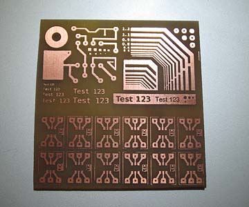
After rinsing and drying the PCB, you can opt to remove the toner immediately, or wait until all other steps. It's somewhat easier to remove the toner before the holes are drilled, but leaving the toner on will protect the copper during the following steps. Whenever you want to do it, use a towel drenched in acetone to wipe away the toner. The next step is drilling the holes, unless you would be brave enough to go for SMD components all the way. For most ordinary component holes, a 0.8mm (1/32") drill is perfect. Larger holes can be 1mm (1/25") or 1.2mm (3/64"). If you don't need to drill many holes, ordinary HSS bits will do. if you're careful enough, you could drill the holes by hand, but a drill press will make your life a lot easier and reduce the risk of breaking the thin bits. If you need to drill many holes, you may want to look for carbide bits because the glass fiber board will wear out HSS bits quickly. Beware: these are extremely brittle, so a stable drill press is essential here.
To improve the looks of your PCB and make soldering easier, you can print a component diagram on the component side, the same way as you transferred the toner on the copper side! This is much easier because the toner sticks even better on the non-copper side. There's no need to waste the glossy paper on this, ordinary office paper will do. Remember to mirror the image before printing. Scrub the surface with acetone (no need to use the abrasive pad), clear out any dirt from the holes, and align the pattern using the drilled holes, holding the board against a bright light. Then, iron as usual, and soak the board in water. Just peel it off, the toner should stick hard enough. Remove any residual paper with the toothbrush.
Before soldering, you'll want to make sure the traces are clean and free of oxide. A quick cleaning with acetone and acid should do. If the PCB is only a disposable prototype, you can simply solder it and use it. However, if it's meant to last longer, you may want to protect it. The most basic protection is to apply no-clean flux to the copper traces. This acts as a kind of varnish which cleans the copper and makes soldering easier. However, in the long term it may wear off. So for those PCBs that really need to last long and/or withstand more extreme environments, you need to protect the copper from oxidizing or a worse fate.
Tin plating makes soldering easier as well, protects the copper, and looks great. Moreover, the process is quite simple: a plating powder exists which needs to be dissolved in water. When submerged in this solution for a few minutes, the pcb is tin-plated automatically. There are a few different products, but the most common one is from Seno, and is called Seno 3211. Now the bad news: this powder ranges from quite to outrageously expensive. For people in the vicinity of Germany, Conrad seems to be the cheapest. The solution has limited life once prepared, so you'll want to make just enough to tin your board. The powder itself has unlimited shelf life if stored properly.
You could also use the classic electrolysis way of tin plating. However, this requires nastier chemicals, and all the copper to be connected to a single cathode. This means you should provide tiny traces on your PCB which connect everything together, and which need to be removed afterwards by scraping or drilling.
Chemical tin plating is nice, but in many cases it's overkill, not worth the expense. As an alternative, you can ‘plate’ the traces yourself with solder. This is easy if you first cover the entire board with flux, you can then almost ‘paint’ the solder on with your soldering iron. Special tinning brush tips exist for soldering irons, which make this process even easier.
Finally, lacquer or varnish will also adequately protect the copper. You could simply solder your board without flux or tin plating, and immediately cover the finished underside with lacquer or varnish. If you use flux to make soldering easier, it may be a good idea to remove it before varnishing, because I'm not sure about how well these two products mix. At any rate, be aware that when spraying varnish or lacquer on the solder, it will probably be hard to solder through the lacquer afterwards. Ideally you should only apply lacquer to the non-soldered areas of the board, but I have no idea how this could be done in a simple way.
Gallery
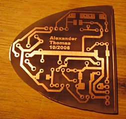
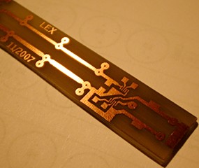
Here are some examples of PCBs I have made with this method.
